| CPC H01L 25/105 (2013.01) [H01L 21/4853 (2013.01); H01L 21/4857 (2013.01); H01L 21/565 (2013.01); H01L 21/568 (2013.01); H01L 21/6835 (2013.01); H01L 21/78 (2013.01); H01L 23/3128 (2013.01); H01L 23/5383 (2013.01); H01L 23/5386 (2013.01); H01L 23/5389 (2013.01); H01L 23/552 (2013.01); H01L 24/19 (2013.01); H01L 24/20 (2013.01); H01L 25/0652 (2013.01); H01L 25/0657 (2013.01); H01L 25/50 (2013.01); H01L 2221/68372 (2013.01); H01L 2224/214 (2013.01); H01L 2225/06506 (2013.01); H01L 2225/06513 (2013.01); H01L 2225/06537 (2013.01); H01L 2225/06562 (2013.01); H01L 2225/06586 (2013.01); H01L 2225/1035 (2013.01); H01L 2225/1052 (2013.01); H01L 2225/1058 (2013.01); H01L 2924/3025 (2013.01)] | 19 Claims |
|
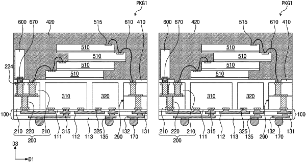
1. A semiconductor package comprising:
a redistribution substrate;
a lower semiconductor chip on the redistribution substrate;
a first conductive structure disposed on the redistribution substrate and laterally spaced apart from the lower semiconductor chip;
a lower molding layer on the lower semiconductor chip and a side surface of the first conductive structure, the lower molding layer exposing an upper surface of the first conductive structure;
a first upper semiconductor chip on the lower molding layer;
a connection terminal electrically connecting the first upper semiconductor chip and the first conductive structure; and
an upper molding layer covering the first upper semiconductor chip,
wherein the connection terminal is directly bonded to the upper surface of the first conductive structure, and
wherein the upper molding layer is in direct contact with the lower molding layer.
|