| CPC H01L 25/0657 (2013.01) [H01L 24/32 (2013.01); H01L 24/73 (2013.01); H01L 25/18 (2013.01); H01L 25/50 (2013.01); H01L 24/33 (2013.01); H01L 24/48 (2013.01); H01L 24/49 (2013.01); H01L 24/83 (2013.01); H01L 24/92 (2013.01); H01L 2224/32059 (2013.01); H01L 2224/32145 (2013.01); H01L 2224/32221 (2013.01); H01L 2224/33181 (2013.01); H01L 2224/48091 (2013.01); H01L 2224/49176 (2013.01); H01L 2224/73215 (2013.01); H01L 2224/73265 (2013.01); H01L 2224/83203 (2013.01); H01L 2224/92165 (2013.01); H01L 2224/92247 (2013.01); H01L 2225/0651 (2013.01); H01L 2225/06506 (2013.01); H01L 2225/06562 (2013.01); H01L 2924/182 (2013.01); H01L 2924/1815 (2013.01)] | 20 Claims |
|
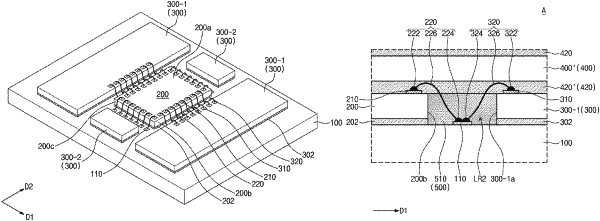
1. A semiconductor package comprising:
a first semiconductor chip on a substrate;
a second semiconductor chip between the substrate and the first semiconductor chip; and
a spacer between the substrate and the first semiconductor chip and spaced apart from the second semiconductor chip,
wherein the substrate includes a first substrate pad between the second semiconductor chip and the spacer,
wherein the second semiconductor chip includes a chip pad on a top surface of the second semiconductor chip and a signal wire extending from the chip pad toward the first substrate pad,
wherein the spacer includes a first dummy pad on a top surface of the spacer and a first dummy wire coupled to the first dummy pad, the first dummy pad being adjacent to the second semiconductor chip,
wherein the first semiconductor chip is attached to the top surface of the second semiconductor chip and the top surface of the spacer by an adhesive layer on a bottom surface of the first semiconductor chip, and
wherein a portion of the signal wire and a portion of the first dummy wire are in the adhesive layer.
|