| CPC H01L 24/96 (2013.01) [H01L 21/561 (2013.01); H01L 21/565 (2013.01); H01L 21/568 (2013.01); H01L 21/78 (2013.01); H01L 24/05 (2013.01); H01L 24/13 (2013.01); H01L 2224/024 (2013.01); H01L 2224/0239 (2013.01); H01L 2224/13024 (2013.01); H01L 2224/13111 (2013.01); H01L 2224/13139 (2013.01); H01L 2224/13144 (2013.01); H01L 2224/13147 (2013.01); H01L 2224/95001 (2013.01); H01L 2924/014 (2013.01); H01L 2924/0105 (2013.01); H01L 2924/01013 (2013.01); H01L 2924/01028 (2013.01); H01L 2924/01029 (2013.01); H01L 2924/01047 (2013.01); H01L 2924/01079 (2013.01); H01L 2924/067 (2013.01); H01L 2924/0695 (2013.01); H01L 2924/07025 (2013.01)] | 11 Claims |
|
1. A packaging structure, comprising:
a substrate;
an adhesive layer formed on the substrate;
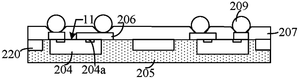
an improvement layer formed on the adhesive layer, wherein the improvement layer includes openings there-in, exposing surface portions of the adhesive layer at bottoms of the openings;
chips located in the openings, wherein the chips include functional surfaces that adhere to the adhesive layer;
an encapsulation layer, on the improvement layer and sidewalls and surfaces of the plurality of chips;
a wiring layer on the functional surfaces and a passivation layer on the wiring layer, wherein the passivation layer has solder openings exposing a portion of the wiring layer; and
solder balls in the solder openings.
|