| CPC H01L 24/73 (2013.01) [H01L 23/49816 (2013.01); H01L 24/06 (2013.01); H01L 24/32 (2013.01); H01L 24/48 (2013.01); H01L 24/49 (2013.01); H01L 25/18 (2013.01); H01L 2224/06102 (2013.01); H01L 2224/32145 (2013.01); H01L 2224/32225 (2013.01); H01L 2224/48148 (2013.01); H01L 2224/48158 (2013.01); H01L 2224/49107 (2013.01); H01L 2224/49109 (2013.01); H01L 2224/49112 (2013.01); H01L 2224/73265 (2013.01); H01L 2924/1431 (2013.01); H01L 2924/1435 (2013.01); H01L 2924/182 (2013.01)] | 20 Claims |
|
1. A semiconductor package comprising:
a package substrate;
a semiconductor chip on the package substrate;
a plurality of first conductive connections connecting the semiconductor chip to the package substrate;
a first spacer and a second spacer on the package substrate, each of the first spacer and the second spacer horizontally spaced apart from the semiconductor chip;
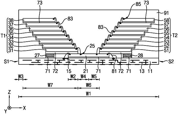
a first tower and a second tower each including a plurality of memory chips, a first memory chip disposed at a lowermost end of the first tower and vertically overlapping the semiconductor chip and the first spacer from a top-down view, and a second memory chip disposed at a lowermost end of the second tower and vertically overlapping the semiconductor chip and the second spacer from a top-down view; and
a plurality of first adhesive layers including an adhesive layer covering a lower surface of the first memory chip and partially covering an upper surface of the semiconductor chip and an adhesive layer covering a lower surface of the second memory chip and partially covering the upper surface of the semiconductor chip.
|