| CPC H01L 24/20 (2013.01) [H01L 23/3157 (2013.01); H01L 2224/211 (2013.01); H01L 2224/2101 (2013.01); H01L 2224/214 (2013.01); H01L 2224/2105 (2013.01); H01L 2924/3511 (2013.01)] | 11 Claims |
|
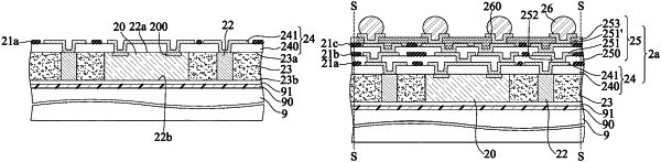
1. A circuit structure, comprising:
a first dielectric layer having a first surface;
a first circuit layer disposed on the first surface of the first dielectric layer;
at least one first metal layer disposed on the first surface of the first dielectric layer and having a plurality of first openings, wherein the first metal layer is a mesh;
a second dielectric layer disposed on the first surface of the first dielectric layer, the first circuit layer and the first metal layer and having a second surface;
a second circuit layer disposed on the second surface of the second dielectric layer; and
at least one second metal layer disposed on the second surface of the second dielectric layer and having a plurality of second openings, wherein the second metal layer is a mesh,
wherein a position of each of the first openings is not aligned with a position of each of the second openings, and the first metal layer and the second metal layer are free from being electrically connected with the first circuit layer and the second circuit layer.
|