| CPC H01L 24/16 (2013.01) [H01L 24/32 (2013.01); H01L 24/48 (2013.01); H01L 2224/0236 (2013.01); H01L 2224/0239 (2013.01); H01L 2224/02331 (2013.01); H01L 2224/02333 (2013.01); H01L 2224/02379 (2013.01); H01L 2224/16225 (2013.01); H01L 2224/32225 (2013.01); H01L 2224/4801 (2013.01); H01L 2224/73265 (2013.01)] | 20 Claims |
|
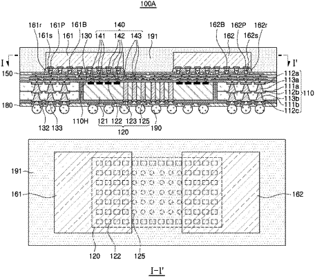
1. A semiconductor package, comprising:
a first semiconductor chip having a first surface and a second surface opposing the first surface, and including first connection pads and second connection pads disposed on the first surface and the second surface, respectively, and through-vias connected to the second connection pads;
a connection structure disposed on the first surface of the first semiconductor chip and including a first redistribution layer electrically connected to the first connection pads of the first semiconductor chip;
a second redistribution layer disposed on the second surface of the first semiconductor chip and electrically connected to the second connection pads of the first semiconductor chip;
a second semiconductor chip disposed on a third surface of the connection structure opposing a fourth surface of the connection structure on which the first semiconductor chip is disposed; and
a third semiconductor chip disposed on the third surface of the connection structure and spaced apart from the second semiconductor chip,
wherein the second semiconductor chip and the third semiconductor chip are respectively disposed to partially vertically overlap with the first semiconductor chip,
wherein in the first semiconductor chip, the first connection pads are disposed not to vertically overlap with the second connection pads,
wherein in the first semiconductor chip, the through-vias and the second connection pads are disposed in a central region of the first semiconductor chip, and the first connection pads are disposed in a peripheral region of the first semiconductor chip, and
wherein the central region of the first semiconductor chip does not vertically overlap with the second semiconductor chip and the third semiconductor chip, a first portion of the peripheral region of the first semiconductor chip vertically overlaps with the second semiconductor chip, and a second portion of the peripheral region of the first semiconductor chip vertically overlaps with the third semiconductor chip.
|