| CPC H01L 24/14 (2013.01) [H01L 21/56 (2013.01); H01L 21/561 (2013.01); H01L 23/3114 (2013.01); H01L 24/96 (2013.01); H01L 2924/0105 (2013.01); H01L 2924/01029 (2013.01)] | 18 Claims |
|
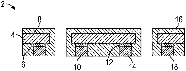
1. A semiconductor package comprising:
a semiconductor die comprising a first side and a second side;
one or more bumps comprised on the first side of the semiconductor die, the one or more bumps comprising a first layer and a second layer directly coupled to the first layer, wherein the first layer comprises a thickness of 10 microns and the second layer comprises a thickness of 20 microns; and
a mold compound encapsulating the semiconductor die on all sides of the semiconductor die, wherein a face of the one or more bumps is exposed through the mold compound;
wherein the first layer is directly coupled to the first side of the semiconductor die.
|