| CPC H01L 24/13 (2013.01) [H01L 24/27 (2013.01); H01L 24/29 (2013.01); H01L 24/32 (2013.01); H01L 24/83 (2013.01); H01L 2224/13005 (2013.01); H01L 2224/13023 (2013.01); H01L 2224/13026 (2013.01); H01L 2224/13078 (2013.01); H01L 2224/279 (2013.01); H01L 2224/29078 (2013.01); H01L 2224/3207 (2013.01); H01L 2224/83895 (2013.01); H01L 2224/83896 (2013.01)] | 19 Claims |
|
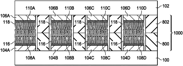
1. A method of forming an electronic device, the method comprising:
providing a first die including a first surface and a second die including a second surface; and
positioning a bond layer positioned between the first surface and the second surface, the bond layer including a set of metallic wires and a dielectric portion, the dielectric portion comprising a polymer matrix and dielectric nanoparticles.
|