| CPC H01L 24/11 (2013.01) [H01L 21/76885 (2013.01); H01L 23/3114 (2013.01); H01L 23/3128 (2013.01); H01L 23/49816 (2013.01); H01L 23/49827 (2013.01); H01L 24/05 (2013.01); H01L 24/13 (2013.01); H01L 2224/023 (2013.01); H01L 2224/0401 (2013.01); H01L 2224/04105 (2013.01)] | 19 Claims |
|
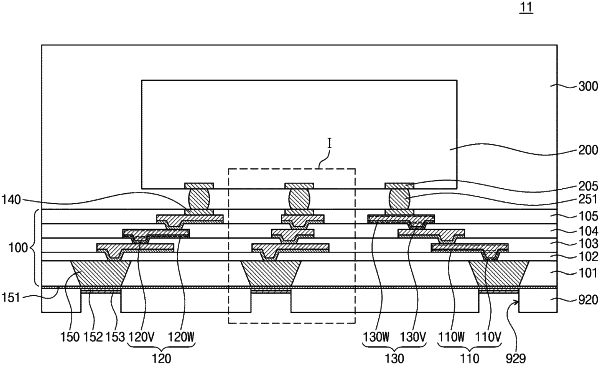
1. A semiconductor package, comprising:
a redistribution substrate; and
a semiconductor chip on a top surface of the redistribution substrate,
wherein the redistribution substrate includes:
an under-bump pattern;
a lower dielectric layer that covers a sidewall of the under-bump pattern; and
a first redistribution pattern on the lower dielectric layer,
wherein the first redistribution pattern includes:
a first conductive layer on a top surface of the lower dielectric layer and including a first tapered via part and a first line part, the first line part extending in a horizontal direction and connected to the first tapered via part; and
a first seed layer between the top surface of the lower dielectric layer and the first conductive layer, the first seed layer covering a bottom surface and side surfaces of the first tapered via part and a bottom surface of the first line part,
wherein a bottom surface of the seed layer covering the first tapered via part directly contacts a top surface of the under-bump pattern,
wherein the top surface of the under-bump pattern is at a vertical level the same as or less than that of the top surface of the lower dielectric layer,
wherein a width at the top surface of the under-bump pattern is greater than a width at a bottom surface of the under-bump pattern,
wherein the under-bump pattern narrows from the top surface of the under-bump pattern to the bottom surface of the under-bump pattern to form a tapered shape having a side surface that extends linearly from the top surface of the under-bump pattern to the bottom surface of the under-bump pattern, and
wherein a thickness of the under-bump pattern is greater than a thickness of the first line part.
|