| CPC H01L 23/562 (2013.01) [H10B 43/27 (2023.02); H10B 43/40 (2023.02)] | 20 Claims |
|
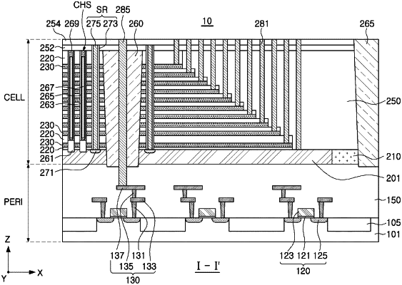
1. A semiconductor device, comprising:
a peripheral circuit region including a lower substrate and circuit elements on the lower substrate;
a first upper substrate and a second upper substrate on the peripheral circuit region;
a first memory cell region on the first upper substrate and a second memory cell region on the second upper substrate; and
at least one cutting region between the first upper substrate and the second upper substrate, the at least one cutting region formed of an insulating material;
wherein each of the first and second memory cell region comprises:
a plurality of gate electrodes stacked in a vertical direction perpendicular to an upper surface of the lower substrate and spaced apart from each other;
a plurality of separation regions penetrating through the plurality of gate electrodes in the vertical direction and extending in a first direction parallel to an upper surface of the lower substrate; and
a plurality of channel structures penetrating through the plurality of gate electrodes and extending in the vertical direction, each of the plurality of channel structures including a channel layer,
wherein the at least one cutting region is disposed between first step-shaped end portions of the plurality of gate electrodes of the first memory cell region and second step-shaped end portions of the plurality of gate electrodes of the second memory cell region,
wherein a height of the at least one cutting region in the vertical direction is greater than at least one of a height of one of the plurality of channel structures in the vertical direction and a height of one of the plurality of separation regions in the vertical direction, and
wherein a bottom of the at least one cutting region is located lower than a bottom of each of the first upper substrate and the second upper substrate.
|