| CPC H01L 23/562 (2013.01) [H01L 24/03 (2013.01); H01L 24/05 (2013.01); H01L 24/13 (2013.01); H01L 24/11 (2013.01); H01L 2224/02125 (2013.01); H01L 2224/03462 (2013.01); H01L 2224/03464 (2013.01); H01L 2224/0401 (2013.01); H01L 2224/05022 (2013.01); H01L 2224/05024 (2013.01); H01L 2224/05027 (2013.01); H01L 2224/05554 (2013.01); H01L 2224/05555 (2013.01); H01L 2224/05556 (2013.01); H01L 2224/05557 (2013.01); H01L 2224/05559 (2013.01); H01L 2224/05572 (2013.01); H01L 2224/1132 (2013.01); H01L 2224/11462 (2013.01); H01L 2224/11464 (2013.01); H01L 2224/11849 (2013.01); H01L 2224/13021 (2013.01); H01L 2224/13023 (2013.01); H01L 2924/3512 (2013.01); H01L 2924/35121 (2013.01)] | 20 Claims |
|
1. A semiconductor device comprising:
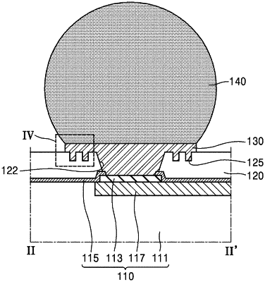
a substrate including a first insulating layer and a conductive layer;
a second insulating layer coating the substrate, the second insulating layer including an opening exposing at least part of the conductive layer and two or more recesses encircling the opening, each of sidewalls of the opening and the recesses being slanted at an obtuse angle with regard to bottoms of the opening and the recesses;
an under-bump metal layer electrically connected to the at least part of the conductive layer;
a via physically contacting both the under-bump metal layer and the at least part of the conductive layer; and
a solder bump on the under-bump metal layer,
wherein the two or more recesses are not physically in contact with the conductive layer,
wherein a depth of the two or more recesses is about 10% to about 90% of a height of the via, and
wherein the two or more recesses are circular trenches surrounding the opening, and a sidewall of the under-bump metal layer is disposed farther from the center of the opening than the sidewalls of the recesses.
|