| CPC H01L 23/562 (2013.01) [H01L 21/76898 (2013.01); H01L 23/481 (2013.01); H01L 24/80 (2013.01); H01L 24/83 (2013.01); H01L 25/0657 (2013.01); H01L 25/50 (2013.01); H01L 2224/80895 (2013.01); H01L 2224/80896 (2013.01); H01L 2224/8385 (2013.01); H01L 2225/06541 (2013.01); H01L 2924/0715 (2013.01); H01L 2924/3511 (2013.01)] | 20 Claims |
|
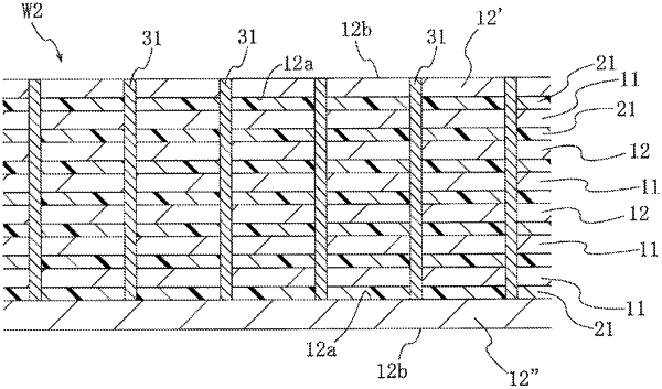
1. A method of manufacturing a semiconductor device, the method comprising:
preparing a plurality of first wafer laminates, each of the first wafer laminates having a laminate configuration, in which a first wafer and a second wafer are included, the first wafer having an element forming surface and a back surface opposite from the element forming surface, and the second wafer having an element forming surface and a back surface opposite from the element forming surface, and the element forming surface sides of the first and second wafers are bonded to each other;
performing thickness reduction, at least twice, to the first wafer of each of the first wafer laminates to form first wafer laminates each having the thinned first wafer; and
bonding the thinned first wafer sides of two first wafer laminates having undergone the thickness reduction to each other to form a second wafer laminate.
|