| CPC H01L 23/552 (2013.01) [H01L 21/324 (2013.01); H10B 43/27 (2023.02); H10B 43/35 (2023.02)] | 9 Claims |
|
1. A semiconductor device comprising:
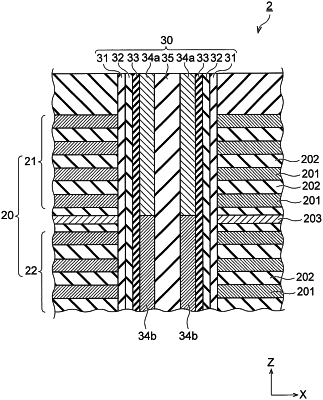
a stacked body comprising first films and second films that are alternately stacked;
a light shielding film provided in a specific layer of the stacked body and having a higher optical absorptivity than that of the second films; and
a channel film extending in the stacked body in a stacking direction, wherein
the channel film comprises a first part located on an upper side than the light shielding film in the stacking direction and containing a monocrystalline semiconductor,
the first films are conductive films,
a material of the first films differs from a material of the light shielding film,
a first plurality of the first films is provided above the light shielding film in the stack,
a second plurality of the first films is provided below the light shielding film in the stack,
the channel film comprises a second part located on a lower side of the light shielding film in the stacking direction and comprises polycrystalline semiconductor, and
the light shielding film is disposed at a position in the stack corresponding to a junction between the first and second parts.
|