| CPC H01L 23/5389 (2013.01) [H01L 25/065 (2013.01)] | 15 Claims |

|
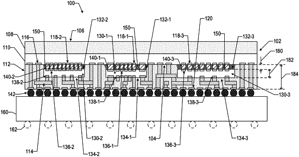
1. A microelectronic assembly, comprising:
a first die having a first face and an opposing second face, the first face including first conductive contacts having a first pitch and arranged in a first pattern, second conductive contacts having a second pitch and arranged in a second pattern, and third conductive contacts having a third pitch and arranged in a third pattern, wherein the second pitch is different than the first pitch, and wherein the third pitch is different than the first pitch and the second pitch;
a second die having a first face and an opposing second face, wherein the second face of the second die includes second conductive contacts having the second pitch and arranged in the second pattern, and wherein respective ones of the second conductive contacts of the second die are electrically coupled to respective ones of the second conductive contacts of the first die;
a third die, having a first face and an opposing second face, wherein the second face of the third die includes third conductive contacts having the third pitch and arranged in the third pattern, and wherein respective ones of the third conductive contacts of the third die are electrically coupled to respective ones of the third conductive contacts of the first die; and
a redistribution layer (RDL) having a first face and an opposing second face, wherein the RDL comprises one or more interconnect structures, wherein the RDL is electrically coupled to the first conductive contacts on the first die, and wherein the second and third dies are between the first die and at least a portion of the RDL.
|
|
5. A microelectronic assembly, comprising:
a redistribution layer (RDL) having a first face and an opposing second face;
a first die at the second face of the RDL, the first die having a first face and an opposing second face, the first face including first conductive contacts having a first pitch and arranged in a first pattern, second conductive contacts having a second pitch and arranged in a second pattern, and third conductive contacts having a third pitch and arranged in a third pattern, wherein the second pitch is different than the first pitch, and wherein the third pitch is different than the first pitch and the second pitch;
a second die, between the first face of the RDL and the first face of the first die, having a first face and an opposing second face, wherein the second face of the second die includes second conductive contacts having the second pitch and arranged in the second pattern, and wherein respective ones of the second conductive contacts of the second die are electrically coupled to respective ones of the second conductive contacts of the first die; and
a third die, between the first face of the RDL and the first face of the first die, having a first face and an opposing second face, wherein the second face of the third die includes third conductive contacts having the third pitch and arranged in the third pattern, and wherein respective ones of the third conductive contacts of the third die are electrically coupled to respective ones of the third conductive contacts of the first die.
|
|
11. A method of manufacturing a microelectronic assembly, comprising:
interconnecting a second die to a first die, the first die including a first face and an opposing second face and the second die including a first face and an opposing second face, wherein the first face of the first die includes first conductive contacts having a first pitch and arranged in a first pattern, second conductive contacts having a second pitch and arranged in a second pattern, and third conductive contacts having a third pitch and arranged in a third pattern, wherein the second pitch is different than the first pitch and the third pitch is different than the first pitch and the second pitch, and wherein the second face of the second die includes second conductive contacts having the second pitch and arranged in the second pattern, and wherein respective ones of the second conductive contacts of the second die are electrically coupled to respective ones of the second conductive contacts of the first die; and
forming a redistribution layer, the redistribution layer comprising a plurality of conductive structures, wherein the second die is between at least a portion of the redistribution layer and the first die.
|