| CPC H01L 23/5383 (2013.01) [H01L 21/4885 (2013.01); H01L 27/0924 (2013.01)] | 7 Claims |
|
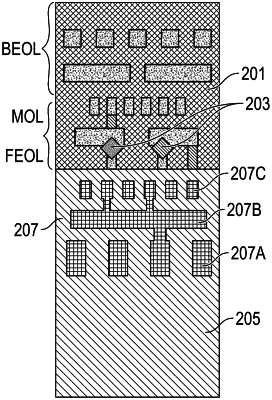
1. A system comprising a monolithic substrate comprising:
a first wiring structure formed fully within bulk material of a semiconductor wafer, wherein the first wiring structure comprises a layer of patterned metal fully within the bulk material of the semiconductor wafer with air gaps above the patterned metal;
one or more active devices formed in an epitaxially grown semiconductor material above the first wiring structure; and
a second wiring structure formed above the one or more active devices.
|