| CPC H01L 23/535 (2013.01) [H10B 12/00 (2023.02)] | 8 Claims |
|
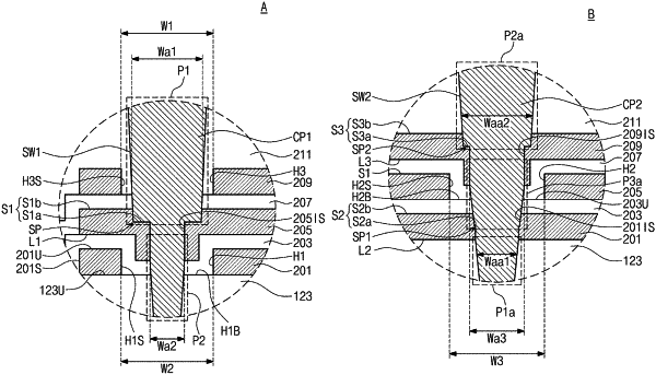
1. A semiconductor device, comprising:
a substrate;
a first electrode on the substrate, the first electrode including a first hole;
a first dielectric layer on the first electrode, the first dielectric layer includes a first portion that extends into the first hole;
a second electrode on the first dielectric layer, the second electrode includes a second portion that fills a remainder of the first hole that is not filled by the first portion of the first dielectric layer;
a second dielectric layer on the second electrode;
a third electrode on the second dielectric layer;
a first contact plug extending through and contacting the first electrode and the third electrode;
a second contact plug extending through the second electrode and contacting the second electrode; and
upper wiring layers on each of the first and second contact plugs,
wherein the first contact plug includes
a first part between a lower surface of the first electrode and an upper surface of the substrate,
a second part between an upper surface of the third electrode and the upper wiring layers, and
a third part between an upper surface of the first electrode and a lower surface of the third electrode,
wherein a sidewall of the first part of the first contact plug is offset to a sidewall of the third part of the first contact plug such that a first discontinuous change in a width of the first contact plug is present between the first and third parts of the first contact plug,
wherein the sidewall of the third part of the first contact plug is offset to a sidewall of the second part of the first contact plug such that a second discontinuous change in the width of the first contact plug is present between the second and third parts of the first contact plug,
wherein the second contact plug includes
a first part between an upper surface of the second electrode and the upper wiring layers, and
a second part between a lower surface of the second electrode and the upper surface of the substrate,
wherein a sidewall of the first part of the second contact plug is offset to a sidewall of the second part of the second contact plug,
wherein the second contact plug extends through the first hole such that the second contact plug extends through the first portion of the first dielectric layer and the second portion of the second electrode, and
wherein the first portion of the first dielectric layer contacts the second contact plug.
|