| CPC H01L 23/5283 (2013.01) [H01L 29/42356 (2013.01); H10B 43/27 (2023.02)] | 20 Claims |
|
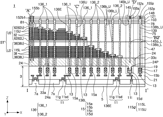
1. A semiconductor device, comprising:
a pattern structure;
a stack structure including a plurality of gate layers stacked and spaced apart from each other in a vertical direction in a first region on the pattern structure and extending into a second region on the pattern structure;
a memory vertical structure penetrating through the stack structure in the first region;
a plurality of gate contact plugs electrically connected to the plurality of gate layers in the second region; and
a first peripheral contact plug spaced apart from the plurality of gate layers,
wherein the plurality of gate layers include a first gate layer,
wherein the plurality of gate contact plugs include a first gate contact plug in contact with and electrically connected to the first gate layer,
wherein each of the plurality of gate contact plugs and the first peripheral contact plug includes a conductive gap fill pattern and a conductive liner layer covering a side surface and a bottom surface of the conductive gap fill pattern,
wherein a side surface of the first gate contact plug and a side surface of the first peripheral contact plug have different numbers of upper bending portions on a level higher than a level of an uppermost gate layer of the plurality of gate layers, and
wherein the number of upper bending portions of a first side of the side surface of the first gate contact plug, disposed in the first direction, is greater than the number of upper bending portions of a first side of the side surface of the first peripheral contact plug, disposed in the first direction, on a level higher than a level of the uppermost gate layer.
|