| CPC H01L 23/528 (2013.01) [H10B 63/30 (2023.02); H10B 63/80 (2023.02); H10N 70/826 (2023.02); H10N 70/841 (2023.02)] | 20 Claims |
|
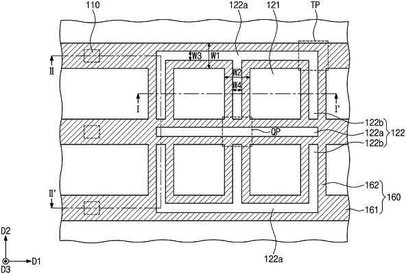
1. A semiconductor device comprising:
a lower layer;
a plurality of first interconnection lines extending in a first direction on the lower layer;
a plurality of second interconnection lines extending in a second direction between the first interconnection lines, and connecting the first interconnection lines, the second direction intersecting the first direction;
first insulating patterns between the second interconnection lines; and
second insulating patterns disposed in the first interconnection lines,
wherein the first interconnection lines include connection regions, to each of which at least one of the second interconnection lines is connected, and
wherein the second insulating patterns extend into the connection regions.
|