| CPC H01L 23/49582 (2013.01) [H01L 21/4821 (2013.01); H01L 23/3107 (2013.01); H01L 23/49541 (2013.01)] | 15 Claims |
|
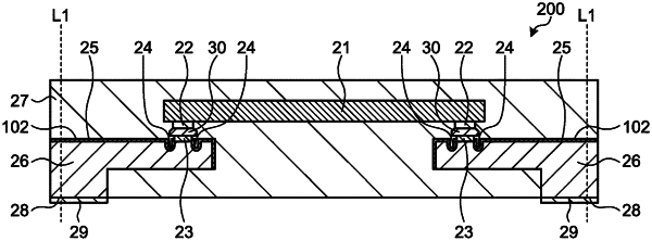
8. A semiconductor device comprising:
a semiconductor element that has a terminal;
a lead portion;
a plating layer that is provided on a connected area of the lead portion and extends to both edges of the lead portion in a width direction of the lead portion, the connected area being an area connected with the semiconductor element;
a pair of recessed portions that face each other across the plating layer on the lead portion and penetrate the lead portion in the width direction;
an oxidized layer that is provided on a surface including the pair of recessed portions of the lead portion;
a solder portion that connects the plating layer and the terminal of the semiconductor element; and
an encapsulation resin that covers the lead portion and the semiconductor element,
wherein a bottom surface of each of the pair of recessed portions is, at a cross-section perpendicular to the width direction, a curved surface, and
an inner edge of each of the pair of recessed portions is coplanar with an outer edge of the plating layer in plan view.
|