| CPC H01L 23/49541 (2013.01) [H01L 23/31 (2013.01); H01L 23/5226 (2013.01)] | 20 Claims |
|
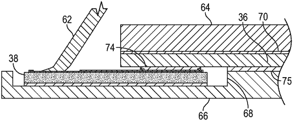
1. A semiconductor package comprising:
a lead frame;
one or more semiconductor die coupled with the lead frame; and
an interposer coupled with the lead frame and with at least one of the one or more semiconductor die;
wherein the interposer comprises an electrically conductive material on a first side of the interposer and an electrically insulative material on a second side of the interposer;
wherein the interposer is coupled with the lead frame through the electrically insulative material such that the electrically conductive material is electrically isolated from the lead frame; and
wherein the electrically conductive material forms at least two separated contact pads.
|