| CPC H01L 23/481 (2013.01) [H01L 21/76898 (2013.01); H01L 23/5283 (2013.01); H01L 23/5286 (2013.01); H01L 25/0657 (2013.01); H01L 2225/06513 (2013.01); H01L 2225/06544 (2013.01); H01L 2225/06586 (2013.01)] | 20 Claims |
|
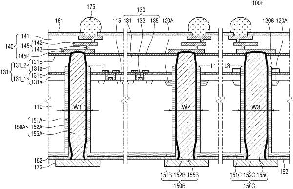
1. A semiconductor device comprising:
a substrate having a first surface and a second surface, opposite to the first surface, a plurality of circuits on the first surface;
an interlayer insulating film on the first surface of the substrate;
an etching delay layer in a region between the first surface of the substrate and the interlayer insulating film;
first and second landing pads on the interlayer insulating film;
a first through electrode penetrating the substrate and the interlayer insulating film, and connected to the first landing pad;
a first electrode insulating film surrounding a sidewall of the first through electrode;
a second through electrode penetrating the substrate, the etching delay layer, and the interlayer insulating film, and connected to the second landing pad, the second through electrode having a width greater than a width of the first through electrode; and
a second electrode insulating film surrounding a sidewall of the second through electrode,
wherein the first and second through electrodes respectively comprise first and second tapered end portions in the interlayer insulating film,
each of the first and second tapered end portions has a cross-sectional shape narrowing closer to the respective ones of the first and second landing pads, and
the first and second electrode insulating films partially extend into the interlayer insulating film such that outer surfaces of the first and second through electrodes are in contact with the interlayer insulating layer in the first and second tapered end portions.
|