| CPC H01L 23/38 (2013.01) [H01L 23/12 (2013.01); H01L 23/3677 (2013.01); H05K 7/20209 (2013.01)] | 20 Claims |
|
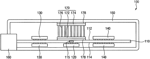
1. A semiconductor module comprising:
a first printed circuit board (PCB);
a plurality of first memory chips on an upper surface and a lower surface of the first PCB;
a control chip on the lower surface of the first PCB;
a heat sink configured to surround the first PCB, the first memory chips and the control chip;
at least one first thermoelectric cooler (TEC) on the upper surface of the first PCB to cool heat from the first PCB;
a first thermal interface material (TIM) between the first TEC and the first PCB, and between the first TEC and the heat sink; and
a first temperature sensor configured to measure a temperature of the first PCB for controlling operations of the first TEC,
wherein a first uneven groove is at an inner surface of the heat sink configured to make contact with the first TEC, the first TIM includes a first uneven portion in the first uneven groove, and the first TEC has an area of no more than about 50% of an area of the first PCB.
|