| CPC H01L 23/3735 (2013.01) [H01L 25/18 (2013.01)] | 21 Claims |
|
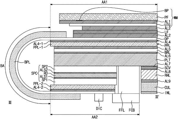
1. A display device comprising:
a display panel including a first area, a bending area, and a second area arranged in a first direction, and comprising a plurality of pixels disposed in the first area;
a driving chip disposed on an upper surface of the second area of the display panel and electrically connected to the plurality of pixels;
a support layer disposed on a lower surface of the first area of the display panel; and
a spacer disposed on the lower surface of the first area of the display panel and overlapping the support layer in plan view, wherein
the spacer comprises:
an upper layer;
a lower layer; and
a base layer disposed between the upper layer and the lower layer and having a thermal conductivity greater than a thermal conductivity of the upper layer and a thermal conductivity of the lower layer;
a first adhesive layer disposed between the upper layer and the base layer;
a second adhesive layer disposed between the lower layer and the base layer; and
the support layer disposed between the spacer and the display panel and including a metal, and
in case that the bending area of the display panel is folded, the spacer overlaps the driving chip in plan view, and
each of the upper layer and the lower layer includes an insulating material,
the support layer has a thermal conductivity greater than the thermal conductivity of the upper layer.
|