| CPC H01L 23/3128 (2013.01) [H01L 23/13 (2013.01); H01L 23/49816 (2013.01); H01L 23/49822 (2013.01); H01L 23/49827 (2013.01); H01L 23/49838 (2013.01); H01L 24/08 (2013.01); H01L 2224/08235 (2013.01)] | 20 Claims |
|
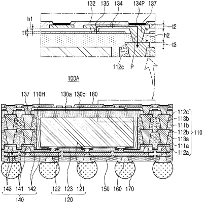
1. A method of manufacturing a fan-out semiconductor package, the method comprising:
forming a frame having a through-hole and including one or more wiring layers;
forming a semiconductor chip in the through-hole of the frame;
forming an encapsulant covering an upper surface of each of the frame and the semiconductor chip, and filling a space between a wall surface of the through-hole of the frame and a side surface of the semiconductor chip;
forming a connection structure below each of the frame and the semiconductor chip, and including one or more redistribution layers;
forming a first metal pattern layer on an upper surface of the encapsulant;
forming an insulating material on the upper surface of the encapsulant and covering the first metal pattern layer; and
forming a second metal pattern layer on an upper surface of the insulating material, a first metal via passing through the insulating material, and a second metal via passing through the insulating material and the encapsulant,
wherein the first metal via electrically connects the first metal pattern layer and the second metal pattern layer, and
wherein the second metal via electrically connects the second metal pattern layer and an uppermost wiring layer among the one or more wiring layers of the frame.
|