| CPC H01L 22/12 (2013.01) [H01L 21/67092 (2013.01); H01L 21/67253 (2013.01); H01L 21/67259 (2013.01); H01L 21/6831 (2013.01); H01L 21/6838 (2013.01); H01L 21/68764 (2013.01); H01L 24/75 (2013.01); H01L 2224/759 (2013.01); H01L 2224/75304 (2013.01); H01L 2224/75725 (2013.01); H01L 2224/75745 (2013.01)] | 25 Claims |
|
1. A substrate bonding apparatus that bonds a first semiconductor substrate and a second semiconductor substrate so that a contact region, in which the first semiconductor substrate and the second semiconductor substrate are in contact, is formed in corresponding parts of the first semiconductor substrate and the second semiconductor substrate, and then the contact region enlarges from the corresponding parts, the substrate bonding apparatus comprising:
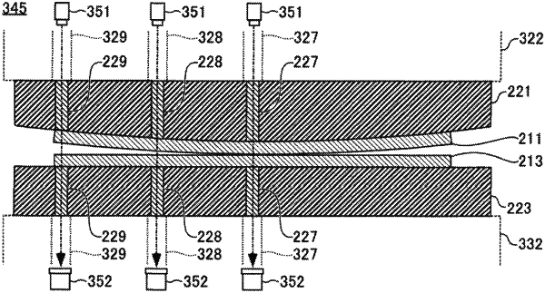
a first substrate holder that holds the first semiconductor substrate and a second substrate holder that holds the second semiconductor substrate, at least one of the first substrate holder and the second substrate holder being provided with a plurality of holes, and one of the first semiconductor substrate and the second semiconductor substrate to be released from the corresponding substrate holder to enlarge the contact region;
a detecting unit that radiates light and detects an optical characteristic of the light that (i) has passed through the at least one of the first substrate holder and the second substrate holder via the plurality of holes and (ii) comes from a surface of the one of the first semiconductor substrate and the second semiconductor substrate to be released, the surface being on an opposite side from a surface, in which the contact region is formed, of the one of the first semiconductor substrate and the second semiconductor substrate to be released, a change in the optical characteristic representing information about the contact region; and
a determining unit that at least one of (i) determines that bonding the first semiconductor substrate and the second semiconductor substrate has been completed, (ii) determines that the first semiconductor substrate and the second semiconductor substrate have become ready to be carried out, and (iii) detects a state of progress of a bonding wave, which indicates a boundary of the contact region, based on the information detected by the detecting unit.
|