| CPC H01L 21/76898 (2013.01) [H01L 21/02068 (2013.01); H01L 21/76831 (2013.01)] | 20 Claims |
|
1. A semiconductor device, comprising:
a first structure comprising:
a first semiconductor substrate;
first transistors on the first semiconductor substrate;
a first interlayered insulating layer covering the first transistors;
first interconnection lines in the first interlayered insulating layer; and
a first metal pattern electrically connected to the first interconnection lines;
a second structure covering the first structure and comprising:
a second interlayered insulating layer covering the first interlayered insulating layer; and
a second semiconductor substrate on the second interlayered insulating layer;
a via hole penetrating the second structure, wherein a top surface of the first metal pattern is exposed by the via hole;
a via insulating layer in the via hole;
a diffusion barrier layer on the via insulating layer; and
a through via in a remaining portion of the via hole and electrically connected to the first metal pattern,
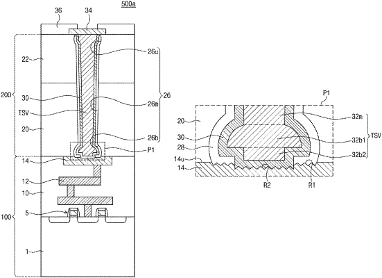
wherein the top surface of the first metal pattern comprises a recess,
the recess comprises a first recess and a second recess, and the second recess is at a center region of a bottom of the first recess, and
a depth of the second recess is deeper than a depth of the first recess.
|