| CPC H01L 21/76898 (2013.01) [H01L 21/76232 (2013.01); H01L 23/481 (2013.01); H01L 24/05 (2013.01); H01L 27/14636 (2013.01); H01L 21/3065 (2013.01); H01L 21/30604 (2013.01); H01L 2224/0557 (2013.01)] | 12 Claims |
|
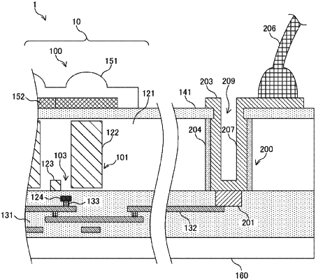
1. A semiconductor device, comprising:
a semiconductor substrate that includes a front surface and a back surface;
a cylindrical insulating film that penetrates the semiconductor substrate;
a wiring layer;
a front surface side pad adjacent to the front surface of the semiconductor substrate;
a conductor layer adjacent to the front surface side pad, wherein
the front surface side pad has a first surface and a second surface,
the first surface is in contact with the conductor layer,
the second surface is in contact with the wiring layer, and
the conductor layer is on an inner side of the cylindrical insulating film; and
a back surface side pad on the back surface of the semiconductor substrate, wherein
the back surface side pad is connected to the front surface side pad via the conductor layer, and
the conductor layer comprises a film that has a same thickness as the back surface side pad.
|