| CPC H01L 21/76895 (2013.01) [H01L 21/0337 (2013.01); H01L 21/32139 (2013.01); H01L 21/7685 (2013.01); H01L 21/76865 (2013.01)] | 18 Claims |
|
1. A semiconductor manufacturing apparatus comprising:
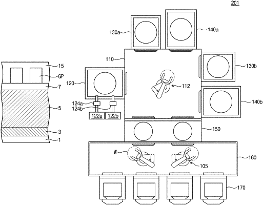
a transfer chamber;
at least one thermally decomposable layer deposition chamber connected to the transfer chamber and configured to deposit a thermally decomposable layer formed of a polymer by supplying a first monomer and a second monomer;
at least one annealing chamber connected to the transfer chamber and configured to decompose the thermally decomposable layer; and
at least one capping layer deposition chamber connected to the transfer chamber and configured to deposit a capping layer,
wherein the thermally decomposable layer is thermally decomposed at a first temperature, the at least one annealing chamber is configured to maintain a third temperature, and the third temperature is higher than the first temperature.
|