| CPC H01L 21/76802 (2013.01) [H01L 21/76814 (2013.01); H01L 21/76843 (2013.01); H01L 21/76855 (2013.01); H01L 29/78666 (2013.01)] | 8 Claims |
|
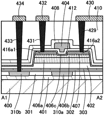
1. A method of fabricating a semiconductor device, comprising:
forming a first insulator over a substrate;
forming a first conductor comprising a metal element and a second conductor over the first insulator, wherein the first conductor and the second conductor are formed from a same film;
forming a second insulator over the first conductor and the second conductor;
forming a semiconductor over the second insulator;
forming a third conductor over the semiconductor as a source or a drain electrode;
forming a third insulator over the third conductor;
forming a fourth conductor as a gate electrode;
forming a fourth insulator over the fourth conductor;
forming a mask layer over the fourth insulator;
forming a first opening in the second insulator, the third insulator, and the fourth insulator to expose a top surface of the first conductor, wherein the first opening is formed by etching the second insulator, the third insulator, and the fourth insulator using plasma and the mask layer as a mask;
performing plasma treatment on at least the first opening, wherein the plasma treatment is performed in an atmosphere containing oxygen;
washing treatment using a liquid in the first opening;
forming a fifth conductor in the first opening;
forming a fifth insulator over the fourth insulator; and
forming a sixth conductor over the fifth insulator,
wherein the sixth conductor is electrically connected to the first conductor through the fifth conductor.
|