| CPC H01L 21/768 (2013.01) [H01L 21/822 (2013.01); H01L 27/04 (2013.01); H01L 27/146 (2013.01); H01L 27/14603 (2013.01); H01L 27/14612 (2013.01); H01L 27/14656 (2013.01); H04N 25/57 (2023.01); H04N 25/621 (2023.01); H04N 25/76 (2023.01)] | 14 Claims |
|
1. An imaging device, comprising:
a pixel comprising:
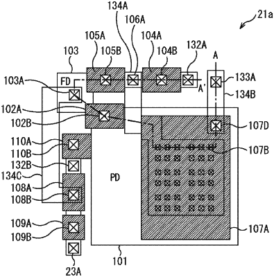
a photoelectric conversion element;
a floating diffusion element;
a capacitance element configured to accumulate a charge from the photoelectric conversion element, wherein
the capacitance element overlaps the photoelectric conversion element,
the capacitance element is electrically connected to the floating diffusion element, and
the capacitance element includes:
a first electrode;
a plurality of trenches in the first electrode; and
a second electrode buried in each trench of the plurality of trenches via a first insulating film, wherein
the first insulating film is between the first electrode and the second electrode; and
a first reset gate and a second reset gate, wherein
the first reset gate is between a power supply and a node connected to the capacitance element, and
the second reset gate is between the floating diffusion element and the node.
|