| CPC H01L 21/76235 (2013.01) [H01L 21/02164 (2013.01); H01L 21/308 (2013.01); H01L 21/324 (2013.01); H01L 21/763 (2013.01); H01L 21/76283 (2013.01); H01L 21/76286 (2013.01); H01L 29/66666 (2013.01)] | 17 Claims |
|
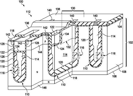
1. A semiconductor device, comprising:
a substrate having a top surface and a bottom surface located opposite from the top surface, the substrate having a semiconductor material between the top surface and the bottom surface;
a shield in a trench in the substrate, the trench extending from the top surface, the shield being electrically conductive, wherein the semiconductor material extends to the trench, wherein the shield is separated from the semiconductor material by a shield liner in the trench, the shield liner being electrically non-conductive;
a metal oxide semiconductor (MOS) transistor, the MOS transistor including:
a gate in the trench and having a gate bottom surface, the shield extending under the gate bottom surface, wherein the gate is electrically isolated from the shield; and
gate dielectric layer in the trench, the gate dielectric layer separating the gate from the semiconductor material; and
an electrically non-conductive shield isolation layer which separates the gate from an angled surface of a contact portion of the shield, the angled surface extending between the gate bottom surface and the top surface of the substrate, the shield isolation layer extending over the substrate top surface, wherein the shield isolation layer does not extend the length of the trench.
|