| CPC H01L 21/32137 (2013.01) [H01L 21/32105 (2013.01); H10B 43/27 (2023.02); H10B 43/35 (2023.02)] | 20 Claims |
|
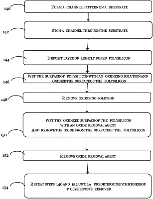
1. A method of processing a substrate, the method comprising:
forming a high aspect ratio (HAR) channel through a substrate, the HAR channel having an aspect ratio greater than 50:1;
depositing a layer of polycrystalline silicon on sidewalls of the HAR channel;
delivering an oxidizing agent into the HAR channel to oxidize uncovered surfaces of the layer of polycrystalline silicon, the oxidizing agent causing formation of an oxidized layer, the oxidized layer having a uniform thickness on the uncovered surfaces of the layer of polycrystalline silicon;
delivering a removal agent into the HAR channel to remove the oxidized layer from the HAR channel; and
repeating steps of oxidizing the uncovered surfaces and removing the oxidized layer until removing a predetermined amount of the layer of polycrystalline silicon.
|