| CPC H01L 21/32136 (2013.01) [C23F 4/00 (2013.01); H01L 21/3065 (2013.01); H01L 21/32139 (2013.01); H01L 23/53228 (2013.01)] | 17 Claims |
|
1. A method of etching a copper (Cu) thin film, the method comprising:
patterning a hard mask layer on the Cu thin film to form a hard mask on the Cu thin film; and
etching the Cu thin film through the hard mask using a plasma of a mixed gas;
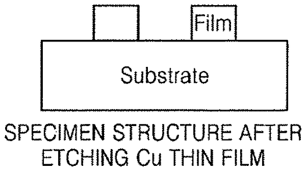
wherein the Cu thin film has a sidewall slope of 70° or greater after the etching, and
wherein the mixed gas includes an inert gas and an organic chelator material including an amine group, the mixed gas not including a halogen gas or a halide gas.
|
|
9. A method of etching a copper (Cu) thin film, the method comprising:
providing the Cu thin film on a substrate;
forming a hard mask layer on the Cu thin film;
etching the hard mask layer to form a hard mask on the Cu thin film; and
plasma etching the Cu thin film through the hard mask using plasma generated from a mixed gas including an inert gas and an organic chelator material including an amine group,
wherein the Cu thin film has a sidewall slope of 70° or greater after the plasma etching.
|