| CPC H01L 21/0268 (2013.01) [C22F 3/02 (2013.01); H01L 21/67115 (2013.01); H01L 23/53214 (2013.01); H01L 23/53228 (2013.01); H01L 29/04 (2013.01); H01L 29/78675 (2013.01); H01L 29/78678 (2013.01)] | 19 Claims |
|
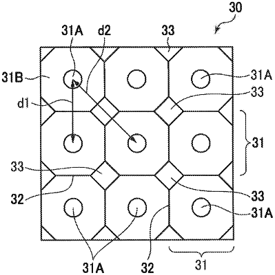
1. A polycrystalline film, comprising:
evenly distributed crystal grains lining up in parallel lines extending along the surface of the film, and
a no-lateral-growth region left at each of locations exposed to both ends of a grain interface, which serves as a partition between the neighboring two crystal grains, in a pattern that exposes the laterally crystallized film after lateral crystal growth, where: one of the both ends of the grain interface is separated from the other in a direction along the surface of the film,
wherein each of the crystal grains is in the shape of a column having a height from the lower surface to the upper surface of the film, and
the crystal grain includes a crystal core in the middle inside its limits within the surface of the film, the crystal core being in the shape of a column having a height from the lower surface to the upper surface of the film.
|