| CPC H01L 21/02304 (2013.01) [H01L 21/02236 (2013.01); H01L 21/02362 (2013.01); H01L 21/02532 (2013.01); H01L 29/16 (2013.01)] | 19 Claims |
|
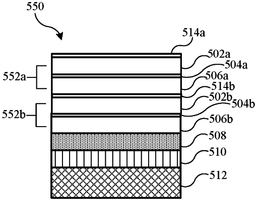
1. A semiconductor processing method comprising:
forming a semiconductor layer stack from pairs of Si-and-SiGe layers, wherein the pairs of Si-and-SiGe layers are formed by:
forming a silicon layer;
forming a germanium barrier layer on the silicon layer, wherein the germanium barrier layer is less than or about 20 Å, and wherein the germanium barrier layer comprises a silicon oxide layer that is formed by exposing the silicon layer to an oxidation plasma generated from an oxidation precursor comprising O2; and
forming a silicon-germanium layer on the germanium barrier layer, wherein the silicon-germanium layer comprises greater than or about 30 at. % germanium.
|