US 11,791,151 B2
Structure production wet etch method and structure production apparatus
Fumimasa Hirikiri, Hitachi (JP)
Assigned to SUMITOMO CHEMICAL COMPANY, LIMITED, Tokyo (JP)
Filed by SUMITOMO CHEMICAL COMPANY, LIMITED, Tokyo (JP)
Filed on Feb. 9, 2022, as Appl. No. 17/668,024.
Application 17/668,024 is a continuation of application No. 17/286,198, granted, now 11,289,322, previously published as PCT/JP2019/040820, filed on Oct. 17, 2019.
Claims priority of application No. 2018-196971 (JP), filed on Oct. 18, 2018; and application No. 2019-138913 (JP), filed on Jul. 29, 2019.
Prior Publication US 2022/0172943 A1, Jun. 2, 2022
Int. Cl. H01L 21/02 (2006.01); H01L 21/306 (2006.01); H01L 21/67 (2006.01); H01S 5/0239 (2021.01)
CPC H01L 21/02019 (2013.01) [H01L 21/30604 (2013.01); H01L 21/67086 (2013.01); H01S 5/0239 (2021.01)] 5 Claims
OG exemplary drawing
 
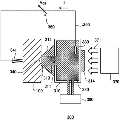
1. A structure production method, comprising:
preparing a wafer at least whose surface is composed of group III nitride crystals and having a non-conductive mask formed on the surface;
preparing an alkaline or acidic etching liquid containing a peroxodisulfate ion as an oxidizing agent that accepts an electron; and
irradiating the surface of the wafer with light, in a state where the surface of the wafer is immersed in the etching liquid heated so as to generate sulfate ion radicals, wherein in the irradiation of the light, the surface of the wafer is intermittently irradiated with the light.