| CPC H01J 37/32642 (2013.01) [H01J 37/32715 (2013.01); H01L 21/67069 (2013.01); H01J 2237/334 (2013.01)] | 15 Claims |

|
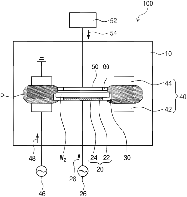
1. A bevel etching apparatus, comprising:
a chuck plate configured to receive a substrate;
a lower ring surrounding a circumference of the chuck plate;
a cover plate on the chuck plate; and
an upper ring surrounding a circumference of the cover plate,
wherein the lower ring includes:
a ring base having constant thickness and configured to support an edge of a bottom surface of the substrate; and
a protrusion extending upwardly from an edge of the ring base to surround a lower portion of a sidewall of the substrate,
wherein the protrusion has an inner diameter greater than an outer diameter of the upper ring,
wherein the protrusion has a height of 745 μm to 772 μm from a top surface of the ring base,
wherein the bevel etching apparatus further comprises a bias electrode comprising a lower electrode and an upper electrode,
wherein an upper surface of the lower electrode is below and spaced apart from the lower ring, and
wherein a lower surface of the upper electrode is above and spaced apart from the lower electrode and the upper ring.
|