| CPC H01H 13/10 (2013.01) [H01H 11/04 (2013.01); H01H 13/183 (2013.01); H01H 13/06 (2013.01); H01H 2229/05 (2013.01)] | 9 Claims |
|
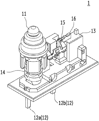
1. A switch device comprising:
a plurality of lead frames that is conductive and configured to be electrically connectable to an external device;
a contact-separation mechanism configured to allow the plurality of lead frames to be electrically connected to and separated from each other; and
an electric element configured to connect the plurality of lead frames to each other, wherein
the electric element is surface-mounted on the plurality of lead frames, and is sealed with resin, and
the plurality of electric elements has a substantially rectangular shape, and is arranged side by side on the plurality of lead frames in a manner in which long sides of one electric element are parallel to those of other electric element.
|