| CPC H01G 4/30 (2013.01) [H01G 4/008 (2013.01); H01G 4/012 (2013.01); H01G 4/1209 (2013.01)] | 12 Claims |
|
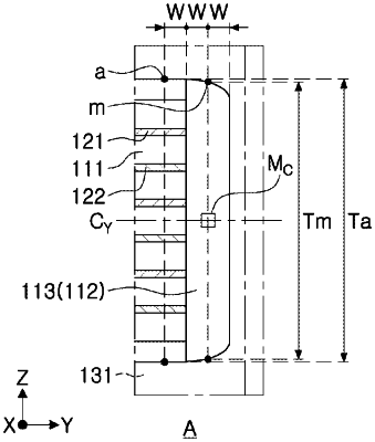
1. A multilayer ceramic electronic component, comprising:
a ceramic body having a capacitance formation portion including first and second surfaces opposing each other in a first direction, third and fourth surfaces opposing each other in a second direction, and fifth and sixth surfaces opposing each other in a third direction, and including a dielectric layer and a first internal electrode and a second internal electrode stacked in the third direction with the dielectric layer interposed therebetween, a first margin portion disposed on the third surface of the capacitance formation portion, and a second margin portion disposed on the fourth surface of the capacitance formation portion;
a first external electrode connected to the first internal electrode; and
a second external electrode connected to the second internal electrode,
wherein a following formula 1 is satisfied,
−0.1≤(Tm−Ta)/Ta, [formula 1]
where in the formula 1, Tm is an average height, in the third direction, of a central region of at least one of the first or second margin portions in the second direction, and Ta is an average height, in the third direction, of an outer region of the capacitance formation portion in the second direction, and
wherein Tm≠Ta.
|