| CPC H01G 4/232 (2013.01) [H01G 4/018 (2013.01); H01G 4/38 (2013.01)] | 20 Claims |
|
1. A film capacitor comprising:
a single film capacitor layer wound around itself in adjacent layers to form a winding, wherein the film capacitor layer comprises:
a single dielectric film having a first side and a second side opposite the first side,
a first metallization layer formed on the dielectric film,
a single dielectric coating formed on a side of the first metallization layer opposite the dielectric film, and
a second metallization layer formed on a side of the dielectric coating opposite the first metallization layer,
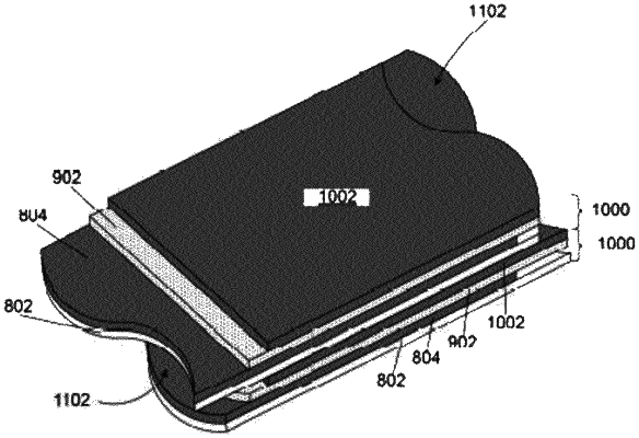
wherein the film capacitor layer has a first outer side comprising the dielectric film, the dielectric coating, and the second metallization layer, and a second outer side opposite the first outer side comprising the dielectric film,
the first outer side and the second outer side being cut in a wave cut such that the first outer side has first alternating areas extending laterally to a first outer edge of the film capacitor layer and second alternating areas curving away from the first outer edge of the film capacitor layer, and the second outer side has first alternating areas extending laterally to a second outer edge of the film capacitor layer and second alternating areas curving away from the second outer edge of the film capacitor layer,
the first alternating areas and the second alternating areas arranged such that alternating edges of the adjacent layers extend laterally to outer edges of the winding, and
wherein the wave cut at the first outer side extends through the second metallization layer, the dielectric coating, and the dielectric film of the film capacitor layer, and wherein the wave cut at the second outer side extends through the dielectric film of the film capacitor layer;
a first metallic contact layer formed on a first outer edge of the winding, and a second metallic contact layer formed on a second outer edge of the winding;
a first terminal formed on an outer edge of the first metallic contact layer, and a second terminal formed on an outer edge of the second metallic contact layer; and
an insulating material encapsulating the winding, the first and second metallic contact layer, and a portion of the first and second terminals.
|