| CPC H01G 4/1227 (2013.01) [C04B 35/4682 (2013.01); H01G 4/012 (2013.01); H01G 4/30 (2013.01); C01P 2002/34 (2013.01); C04B 2235/78 (2013.01)] | 38 Claims |
|
1. A ceramic electronic component comprising:
a body including dielectric layers and internal electrodes; and
external electrodes disposed on the body and connected to the internal electrodes,
wherein the dielectric layer includes a plurality of dielectric crystal grains,
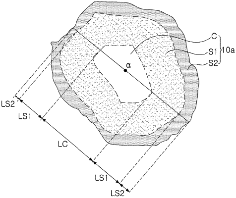
at least one of the plurality of dielectric crystal grains has a core-double shell structure comprising a core and a double shell,
the double shell of the core-double shell structure includes a first shell surrounding at least a portion of the core and a second shell surrounding at least a portion of the first shell,
the first shell includes one or more of a first element selected from the group consisting of Sn, Sb, Ge, Si, Ga, In, and Zr, and
the second shell includes a second element of one or more of Ca or Sr.
|