| CPC G11C 29/88 (2013.01) [G06F 11/2094 (2013.01); G06F 12/10 (2013.01); G11C 17/16 (2013.01); G11C 17/18 (2013.01); G06F 2201/82 (2013.01)] | 19 Claims |
|
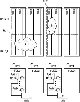
1. A memory device, comprising:
a first bank including first wordlines;
a second bank including second wordlines;
a third bank including third wordlines;
a first fuse circuit configured to receive a first row address indicating a wordline among the first wordlines and the second wordlines, and perform a first repair operation with a first repair unit when the first row address matches stored failed addresses;
a second fuse circuit configured to receive a second row address indicating a wordline among the third wordlines, and perform a second repair operation with a second repair unit when the second row address matches the stored failed addresses; and
wherein the first repair unit is a 2n-wordline pair unit and the second repair unit is a 2-wordline pair unit, where “n” is a positive integer greater than one.
|