| CPC G11C 16/349 (2013.01) [G11C 7/04 (2013.01); G11C 16/10 (2013.01); G11C 16/26 (2013.01); G11C 16/30 (2013.01); G11C 16/32 (2013.01); G11C 16/3404 (2013.01); G11C 16/3459 (2013.01)] | 20 Claims |
|
1. A method, comprising:
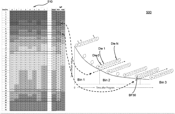
associating, by a processing device, a set of dies of a block family with a die family, wherein the block family is associated with a first threshold voltage offset bin for voltage offsets to be applied in a read operation; and
responsive to detecting a triggering event, associating each die of the set of dies with a second threshold voltage offset bin for voltage offsets to be applied in a read operation, wherein the second threshold voltage offset bin is selected based on a representative die of the set of dies associated with the die family.
|