| CPC G11C 16/3445 (2013.01) [G11C 11/5678 (2013.01); G11C 13/004 (2013.01); G11C 13/0069 (2013.01); G11C 16/16 (2013.01); G11C 16/26 (2013.01)] | 20 Claims |
|
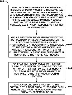
1. A method for erasing a plurality of two-terminal memory cells, comprising:
applying a first erase process to a plurality of two-terminal memory cells of a device;
applying a first read process to the plurality of two-terminal memory cells and verifying the plurality of two-terminal memory cells are in an unprogrammed state;
applying a weak program process to the plurality of two-terminal memory cells;
applying a second read process to determine whether a memory cell of the plurality of two-terminal memory cells is in a programmed state in response to the weak program process; and
applying a second erase process to the memory cell in response to determining that the memory cell is in the programmed state.
|