| CPC G11C 16/10 (2013.01) [G11C 11/5628 (2013.01); G11C 11/5671 (2013.01); G11C 16/0483 (2013.01); G11C 16/08 (2013.01); G11C 16/26 (2013.01); G11C 16/3459 (2013.01); H10B 41/10 (2023.02); H10B 41/27 (2023.02); H10B 43/10 (2023.02); H10B 43/27 (2023.02)] | 13 Claims |
|
1. A storage device, comprising:
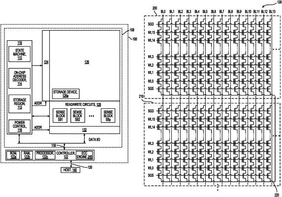
a non-volatile memory including a control circuitry that is communicatively coupled to a memory block that includes an array of memory cells which are arranged in a plurality of word lines, wherein the control circuitry is configured to program the memory cells of the plurality of word lines in a plurality of programming loops, the programming loops including:
applying a programming pulse to a selected word line of the plurality of word lines to program at least one memory cell of the selected word line to a programmed data state; and
simultaneously applying a verify pulse to the selected word line to verify a data state being programmed, applying a first voltage to at least one unselected word line that has not been programmed, and applying a second voltage to at least one unselected word line that has already been programmed, the first voltage being determined as a function of the programmed data state to reduce a voltage threshold distribution across the memory cells in the memory block.
|