| CPC G11C 13/0038 (2013.01) [G05F 3/262 (2013.01); G11C 13/004 (2013.01); G11C 13/0004 (2013.01); G11C 13/0026 (2013.01); G11C 13/0028 (2013.01); G11C 13/0069 (2013.01); G11C 13/003 (2013.01); G11C 2013/0045 (2013.01); G11C 2013/0078 (2013.01); G11C 2213/72 (2013.01)] | 15 Claims |
|
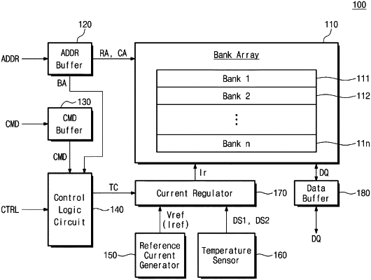
1. A nonvolatile memory device comprising:
a memory cell array including a plurality of memory cells;
a temperature sensor configured to sense a temperature and to generate a first differential signal and a second differential signal which are based on the sensed temperature;
a reference current generator configured to generate a reference current;
a current mirror circuit configured to generate a first compensation current and a second compensation current corresponding to a difference value between the first and second differential signals, to copy a first current that is a sum of the reference current and the first compensation current to generate a second current having a same value as a value of the first current, and to regulate the reference current depending on a difference value of the second current and the second compensation current; and
a write driver configured to drive a bit line or a word line connected to the memory cell array based on the regulated reference current.
|