| CPC G11C 11/5642 (2013.01) [G06F 11/1068 (2013.01); G11C 11/5671 (2013.01); G11C 16/0483 (2013.01); G11C 16/26 (2013.01); G11C 16/08 (2013.01); G11C 16/30 (2013.01); G11C 2211/563 (2013.01); G11C 2211/5642 (2013.01); H10B 43/27 (2023.02); H10B 43/35 (2023.02)] | 20 Claims |
|
1. A memory system comprising:
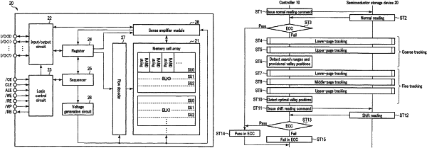
a semiconductor storage device including a plurality of memory cells and a word line being connected to the plurality of memory cells, each of the plurality of memory cells being capable of storing data of n bits (n is an integer equal to or larger than 3); and
a memory controller configured to control the semiconductor storage device,
wherein
the memory controller is further configured to send a first read request,
in response to the first read request, the semiconductor storage device is configured to perform a first read operation of reading first data out of the plurality of memory cells with a first voltage applied to the word line,
the memory controller is further configured to send a second read request,
in response to the second read request, the semiconductor storage device is configured to perform a second read operation of reading second data out of the plurality of memory cells with a second voltage within a first voltage range and a third voltage within a second voltage range applied to the word line, perform a first logical operation of logically processing the first data and the second data, and send third data generated by the first logical operation to the memory controller,
the first voltage range is smaller than the first voltage, and
the second voltage range is larger than the first voltage.
|