| CPC G11C 11/4093 (2013.01) [G11C 5/06 (2013.01); G11C 5/14 (2013.01); G11C 11/4074 (2013.01); G11C 11/4085 (2013.01)] | 17 Claims |
|
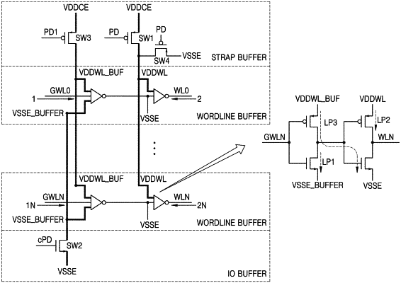
1. A wordline driver circuit for a random-access memory (RAM) configured to reduce leakage during a power down mode, the wordline driver circuit comprising:
a pre-driver stage comprising:
a strap buffer defining a header and comprising a first switch that is configured to connect a first set of wordlines to a first voltage; and
an input-output buffer defining a footer and comprising a second switch that is configured to connect a second set of wordlines to a second voltage,
wherein the strap buffer further comprises a third switch that is connected between inverters and the first voltage and is configured to connect the second set of wordlines to the first voltage.
|