| CPC G11C 11/4085 (2013.01) [G11C 7/1063 (2013.01); G11C 11/4074 (2013.01); G11C 11/4096 (2013.01)] | 19 Claims |
|
1. A memory device, comprising:
a memory block coupled to a plurality of local word lines;
a peripheral circuit configured to couple the plurality of local word lines to a plurality of global word lines through a pass switch circuit and configured to perform a read operation on the memory block; and
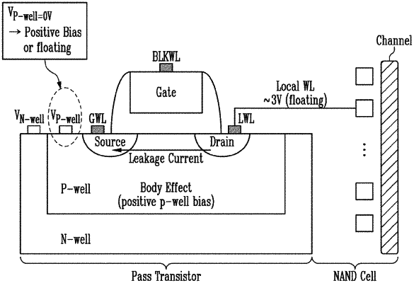
control logic configured to control the peripheral circuit to cause or increase a leakage current of the pass switch circuit, and discharge potential levels of the plurality of local word lines using the leakage current of the pass switch circuit when the memory device enters a ready state after the read operation,
wherein the leakage current of the pass switch circuit is caused or increased by applying a positive voltage to, or floating body regions of a plurality of pass transistors in the pass switch circuit.
|