US 11,790,962 B2
Strobe acquisition and tracking
Bret Stott, Menlo Park, CA (US); Frederick A. Ware, Los Altos Hills, CA (US); Ian P. Shaeffer, Los Gatos, CA (US); and Yuanlong Wang, Sunnyvale, CA (US)
Assigned to RAMBUS INC., San Jose, CA (US)
Filed by Rambus Inc., San Jose, CA (US)
Filed on Jul. 12, 2021, as Appl. No. 17/305,654.
Application 17/305,654 is a continuation of application No. 16/459,330, filed on Jul. 1, 2019, granted, now 11,062,748.
Application 16/459,330 is a continuation of application No. 15/665,312, filed on Jul. 31, 2017, granted, now 10,339,990, issued on Jul. 2, 2019.
Application 15/665,312 is a continuation of application No. 15/017,415, filed on Feb. 5, 2016, granted, now 9,721,630, issued on Aug. 1, 2017.
Application 15/017,415 is a continuation of application No. 13/959,633, filed on Aug. 5, 2013, granted, now 9,257,163, issued on Feb. 9, 2016.
Application 13/959,633 is a continuation of application No. 12/520,068, granted, now 8,504,788, issued on Aug. 6, 2013, previously published as PCT/US2007/088244, filed on Dec. 19, 2007.
Claims priority of provisional application 60/876,408, filed on Dec. 20, 2006.
Prior Publication US 2022/0084571 A1, Mar. 17, 2022
This patent is subject to a terminal disclaimer.
Int. Cl. G11C 7/22 (2006.01); G06F 13/16 (2006.01); G11C 7/02 (2006.01)
CPC G11C 7/222 (2013.01) [G06F 13/1689 (2013.01); G11C 7/02 (2013.01); G11C 7/22 (2013.01)] 20 Claims
OG exemplary drawing
 
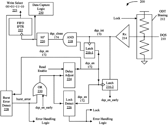
1. A memory controller, comprising:
an interface to receive a data strobe signal and corresponding read data, wherein the data strobe signal and the read data correspond to a read command issued by the memory controller, and wherein the read data is received in accordance with the data strobe signal;
data receive circuitry, including gate logic to gate the data strobe signal with an internally generated data strobe enable signal to generate a clean data strobe signal, and data capture logic responsive to the clean data strobe signal to capture the read data;
burst error detection circuitry to generate a burst error signal indicating whether a count of edges of the clean data strobe signal during a memory read is equal to a predefined value; and
data strobe adjust circuitry to adjust timing of the internally generated data strobe enable signal in accordance with a value of the burst error signal.